توضیحات محصول:
مونتاژ PCB ارتباطی یک راهحل بسیار پیشرفته و قابل اعتماد است که برای پاسخگویی به نیازهای سختگیرانه زیرساختهای ارتباطی مدرن طراحی شده است. این محصول به دلیل کیفیت ساخت استثنایی خود، که شامل مواد و تکنیکهای تولید پیشرفته برای اطمینان از عملکرد بهینه حتی در چالشبرانگیزترین محیطها است، متمایز است. این مونتاژ که با دقت مهندسی شده است، برای کاربردهایی که به قابلیتهای ارتباطی قوی همراه با توانایی مدیریت کارآمد بارهای جریان سنگین نیاز دارند، ایدهآل است.
یکی از ویژگیهای تعیینکننده این مونتاژ PCB ارتباطی، گزینههای پرداخت سطح آن است. این محصول با پرداختهای ENIG (نیکل بدون الکترولیز غوطهوری طلا) و HASL (تراز کردن لحیم هوای گرم) بدون سرب در دسترس است که قابلیت لحیمکاری عالی و محافظت برتر در برابر اکسیداسیون و خوردگی را فراهم میکند. پرداخت ENIG، به ویژه، به دلیل سطح صاف و عملکرد قابل اعتماد در مدارهای ارتباطی با فرکانس بالا، مورد توجه است و آن را به انتخابی عالی برای کاربردهای پیشرفته HDI PCB تبدیل میکند. پرداخت HASL بدون سرب، انطباق با استانداردهای زیستمحیطی را در عین حفظ خواص مکانیکی و الکتریکی عالی تضمین میکند.
این مونتاژ از حداقل قطر سوراخ 0.1 میلیمتر پشتیبانی میکند و امکان ایجاد اتصالات با چگالی بالا را فراهم میکند که در دستگاههای ارتباطی مدرن ضروری هستند. این قابلیت حفاری دقیق، امکان ادغام طرحهای مدار پیچیده را فراهم میکند و از روند کوچکسازی در سختافزار زیرساختهای ارتباطی پشتیبانی میکند. قطر سوراخ کوچک، همراه با تکنیکهای تولید پیشرفته PCB، تضمین میکند که مونتاژ میتواند الزامات مسیریابی و لایهبندی پیچیده را بدون به خطر انداختن یکپارچگی سیگنال یا استحکام مکانیکی برآورده کند.
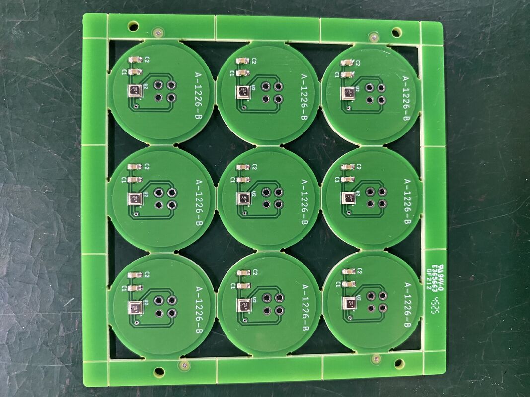
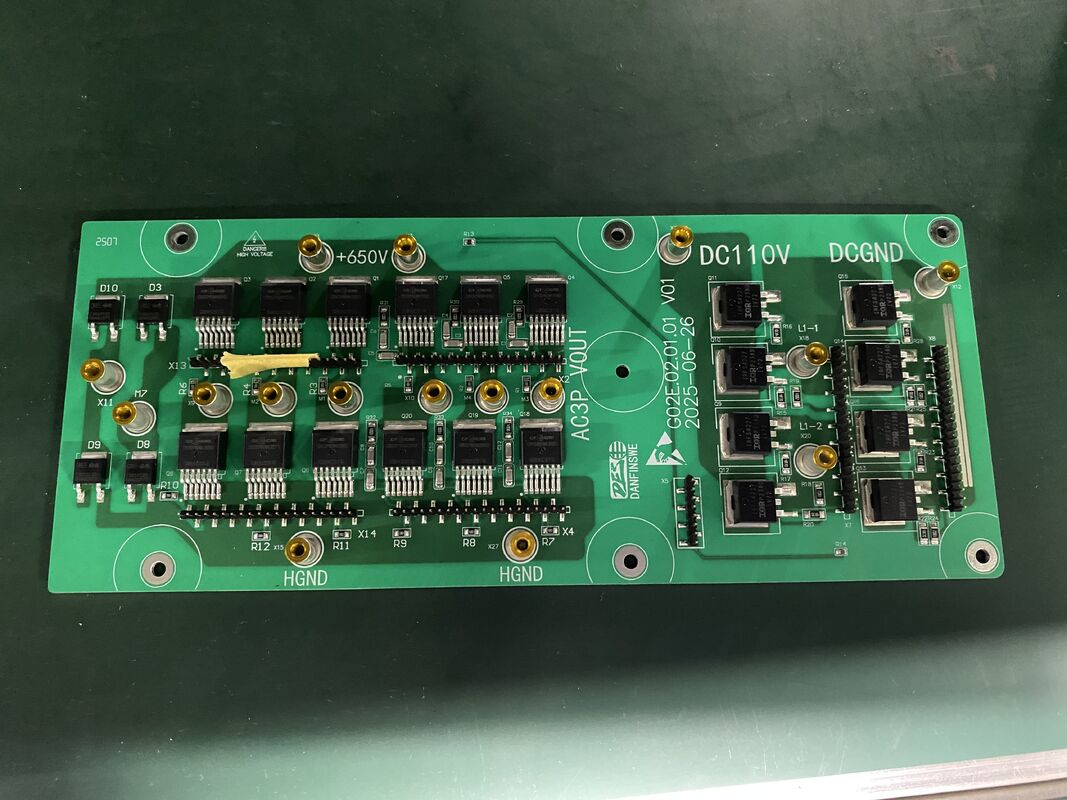
علاوه بر این، این محصول دارای انواع مختلفی از طریقها، از جمله طریقهای سوراخدار، کور و مدفون است. این انواع طریقها در طرحهای HDI PCB حیاتی هستند، زیرا اتصالات چند لایه را تسهیل میکنند و عملکرد کلی الکتریکی برد را افزایش میدهند. طریقهای سوراخدار اتصالات مکانیکی قوی را فراهم میکنند و برای اجزایی که به اتصالات لحیم قوی نیاز دارند، ایدهآل هستند. طریقهای کور لایههای بیرونی را به لایههای داخلی متصل میکنند بدون اینکه از کل برد عبور کنند، در نتیجه فضا را ذخیره کرده و طول مسیر سیگنال را کاهش میدهند. طریقهای مدفون فقط لایههای داخلی را متصل میکنند و طرح برد را بیشتر بهینه میکنند و امکان تراکم مدار بالاتر را فراهم میکنند. این ترکیب از انواع طریقها، مونتاژ PCB ارتباطی را قادر میسازد تا یکپارچگی سیگنال و قابلیت اطمینان بالاتری را ارائه دهد که برای کاربردهای جریان سنگین در سیستمهای زیرساختهای ارتباطی ضروری است.
ضخامت برد این مونتاژ از 0.2 میلیمتر تا 6 میلیمتر متغیر است و انعطافپذیری را برای پاسخگویی به نیازهای مختلف کاربردی ارائه میدهد. بردهای نازکتر برای دستگاههای جمع و جور و سبک وزن ایدهآل هستند، در حالی که بردهای ضخیمتر دوام بیشتری را فراهم میکنند و از بارهای جریان سنگین پشتیبانی میکنند. این طیف گسترده در انتخاب ضخامت تضمین میکند که مونتاژ میتواند برای پاسخگویی به نیازهای مکانیکی و الکتریکی خاص تنظیم شود و آن را برای طیف وسیعی از پروژههای زیرساختهای ارتباطی مناسب میسازد.
در هسته این محصول فناوری HDI PCB قرار دارد که مخفف عبارت High-Density Interconnect Printed Circuit Board است. HDI PCBها به دلیل تراکم مدار برتر، عملکرد الکتریکی پیشرفته و مزایای صرفهجویی در فضا شناخته شدهاند. استفاده از فناوری HDI در این مونتاژ PCB ارتباطی امکان ادغام مدارهای پیچیده را در یک فرم فشرده فراهم میکند و انتقال سیگنال سریعتر و کاهش مصرف انرژی را امکانپذیر میسازد. این امر به ویژه در زیرساختهای ارتباطی که انتقال داده کارآمد و مدیریت جریان سنگین قابل اعتماد از اهمیت بالایی برخوردار است، مهم است.
این مونتاژ که برای مقاومت در برابر شرایط سخت کاربردهای جریان سنگین طراحی شده است، عملکرد پایدار و بدون وقفه را در سیستمهای زیرساختهای ارتباطی تضمین میکند. توانایی مدیریت بارهای جریان سنگین بدون کاهش عملکرد یا قابلیت اطمینان، آن را به یک جزء ضروری برای تجهیزات ارتباطی پرمصرف تبدیل میکند. چه در ایستگاههای پایه، روترهای شبکه یا سایر اجزای زیرساختهای حیاتی استفاده شود، این مونتاژ PCB ارتباطی عملکرد قابل اعتمادی را که برای حفظ اتصال یکپارچه مورد نیاز است، ارائه میدهد.
به طور خلاصه، مونتاژ PCB ارتباطی یک راهحل پیشرفته است که گزینههای پرداخت سطح پیشرفته مانند ENIG و HASL بدون سرب، حداقل قطر سوراخ 0.1 میلیمتر، انواع مختلف طریقها از جمله سوراخدار، کور و مدفون، و طیف وسیعی از ضخامت برد از 0.2 میلیمتر تا 6 میلیمتر را ترکیب میکند. این محصول که بر اساس فناوری HDI PCB ساخته شده است، به طور خاص برای پشتیبانی از الزامات جریان سنگین در زیرساختهای ارتباطی طراحی شده است و قابلیت اطمینان، دوام و عملکرد الکتریکی استثنایی را ارائه میدهد. این امر آن را به انتخابی ایدهآل برای مهندسان و تولیدکنندگانی تبدیل میکند که به دنبال یک مونتاژ PCB با کیفیت بالا هستند که قادر به پاسخگویی به چالشهای سخت سیستمهای ارتباطی مدرن باشد.
ویژگیها:
- نام محصول: مونتاژ PCB ارتباطی
- سازنده: سازنده قابل اعتماد و با تجربه که استانداردهای با کیفیت بالا را تضمین میکند
- لایه های PCB: 6 لایه برای طرح های مدار پیچیده
- کنترل امپدانس: بله، برای یکپارچگی سیگنال بهینه
- ضخامت برد: 0.2-6 میلیمتر مناسب برای نیازهای مختلف کاربردی
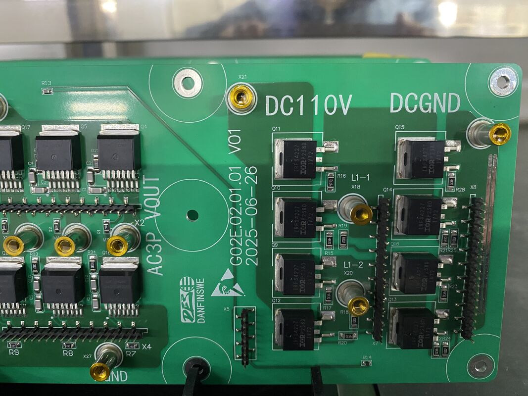
- مس ضخیم: از ظرفیت جریان سنگین و دوام بیشتر پشتیبانی میکند
- محافظت در برابر نوسانات: یکپارچه برای محافظت از اجزای ارتباطی حساس
- بسته بندی بیرونی: بسته بندی کارتن برای حمل و نقل ایمن و مطمئن
پارامترهای فنی:
| نام محصول |
مونتاژ PCB ارتباطی |
| نوع طریق |
سوراخدار، کور، مدفون |
| سفارشی |
بله |
| پرداخت سطح |
ENIG، HASL بدون سرب |
| زمینه کاربرد |
ارتباطات 5G |
| ضخامت برد |
0.2-6 میلیمتر |
| کنترل امپدانس |
بله |
| حداقل قطر سوراخ |
0.1 میلیمتر |
| PCB ارتباطی |
High Tg170 و High Tg180 |
| بسته بندی بیرونی |
کارتن |
کاربردها:
مونتاژ PCB ارتباطی یک جزء ضروری است که به طور خاص برای کاربردهای زیرساختهای ارتباطی قوی طراحی شده است. اندازه PCB سفارشی آن امکان انعطافپذیری در طراحی را فراهم میکند و اطمینان حاصل میکند که نیازهای منحصر به فرد دستگاهها و سیستمهای ارتباطی مختلف را برآورده میکند. این محصول برای استفاده در محیطهایی که ارتباط قابل اعتماد و با عملکرد بالا حیاتی است، مانند مراکز داده، هابهای مخابراتی و نصب تجهیزات شبکه، ایدهآل است.
یکی از موارد کاربرد کلیدی برای این مونتاژ PCB ارتباطی، در توسعه و نگهداری زیرساختهای ارتباطی پیشرفته است. این مونتاژ از طریقهای سوراخدار، کور و مدفون پشتیبانی میکند و طرحهای چند لایه پیچیده را که یکپارچگی سیگنال و قابلیت اطمینان را افزایش میدهند، امکانپذیر میسازد. این تطبیقپذیری آن را برای استفاده در روترها، سوئیچها و سایر سختافزارهای شبکه که عملکرد الکتریکی دقیق و دوام را طلب میکنند، مناسب میسازد.
گزینههای پرداخت سطح محصول، از جمله ENIG و HASL بدون سرب، قابلیت لحیمکاری عالی و مقاومت در برابر خوردگی را تضمین میکنند که برای عملکرد طولانیمدت در شرایط محیطی سخت یا متغیر حیاتی هستند. علاوه بر این، مونتاژ PCB با استانداردهای کیفیت ROHS مطابقت دارد و محصولی سازگار با محیط زیست را تضمین میکند که استانداردهای بینالمللی ایمنی و بهداشت را برآورده میکند.
لایه های مسی ضخیم یک ویژگی برجسته در این مونتاژ PCB هستند که ظرفیت حمل جریان برتر و مدیریت حرارتی پیشرفته را فراهم میکنند. این امر آن را برای دستگاههای ارتباطی پرمصرف که به اتلاف گرما و عملکرد الکتریکی پایدار نیاز دارند، عالی میکند. مس ضخیم همچنین به استحکام مکانیکی PCB کمک میکند و دوام را در سناریوهای کاربردی سخت تضمین میکند.
بستهبندی بیرونی از مواد مقوایی محکم ساخته شده است که محافظت قابل اعتمادی را در هنگام حمل و نقل و جابجایی ارائه میدهد. این امر تضمین میکند که مونتاژهای PCB در شرایط عالی میرسند و آماده ادغام فوری در سیستمهای ارتباطی هستند.
به طور خلاصه، مونتاژ PCB ارتباطی برای طیف گستردهای از سناریوهای کاربردی در بخش زیرساختهای ارتباطی مناسب است. اندازه PCB قابل تنظیم، قابلیتهای چندگانه طریق از جمله طریقهای سوراخدار، کور و مدفون، انطباق با ROHS و گزینههای پرداخت سطح برتر، آن را به انتخابی قابل اعتماد تبدیل میکند. گنجاندن لایههای مسی ضخیم، مناسب بودن آن را برای تجهیزات ارتباطی با عملکرد بالا و بادوام که در محیطهای شبکه حیاتی استفاده میشوند، بیشتر میکند.
سفارشی سازی:
محصول مونتاژ PCB ارتباطی ما خدمات سفارشیسازی جامعی را برای پاسخگویی به نیازهای خاص شما ارائه میدهد. با کنترل امپدانس دقیق، ما یکپارچگی سیگنال بهینه را تضمین میکنیم که برای کاربردهای ارتباطی 5G با فرکانس بالا حیاتی است. مشتریان میتوانند از میان انواع رنگهای ماسک لحیم، از جمله آبی، سبز و سایر موارد، برای مطابقت با ترجیحات طراحی خود انتخاب کنند.
به عنوان یک تولید کننده قابل اعتماد، ما به شدت به سیستم کیفیت ROHS پایبند هستیم و مونتاژهای PCB سازگار با محیط زیست و با کیفیت بالا را تضمین میکنیم. PCBهای ارتباطی ما با مواد High Tg170 و High Tg180 ساخته شدهاند که پایداری حرارتی و دوام عالی را برای محیطهای سخت فراهم میکنند.
PCBهای ما که برای پشتیبانی از بارهای جریان سنگین و شامل ویژگیهای محافظت در برابر نوسانات پیشرفته طراحی شدهاند، برای سیستمهای ارتباطی قوی ایدهآل هستند. به راهحلهای سفارشی ما اعتماد کنید تا عملکرد و قابلیت اطمینان دستگاههای ارتباطی 5G شما را افزایش دهید.
پشتیبانی و خدمات:
محصول مونتاژ PCB ارتباطی ما با پشتیبانی و خدمات فنی جامع پشتیبانی میشود تا عملکرد و قابلیت اطمینان بهینه را تضمین کند. ما اسناد دقیقی از جمله دستورالعملهای مونتاژ، روشهای آزمایش و راهنماهای عیبیابی ارائه میدهیم تا ادغام و نگهداری روان را تسهیل کنیم.
تیم پشتیبانی فنی با تجربه ما آماده است تا در مورد سوالات طراحی، انتخاب اجزا و بهینهسازی فرآیند برای پاسخگویی به نیازهای خاص برنامه ارتباطی شما کمک کند. ما خدمات تست سفارشی را برای تأیید یکپارچگی سیگنال، تطبیق امپدانس و عملکرد کلی مونتاژهای PCB ارائه میدهیم.
علاوه بر این، ما خدمات تعمیر و بازسازی را برای رسیدگی به هرگونه مشکلی که ممکن است در طول چرخه عمر محصول ایجاد شود، ارائه میدهیم و حداقل زمان خرابی و راندمان عملیاتی پایدار را تضمین میکنیم. تعهد ما به کیفیت و رضایت مشتری در هر مرحله از استفاده از محصول گسترش مییابد.
برای پشتیبانی مداوم، ما بهروزرسانیهای نرمافزاری و ارتقاء میانافزار را در صورت لزوم، و همچنین جلسات آموزشی برای کمک به تیم شما برای به حداکثر رساندن مزایای راهحلهای مونتاژ PCB ارتباطی خود ارائه میدهیم.
بسته بندی و حمل و نقل:
محصولات مونتاژ PCB ارتباطی ما با دقت بستهبندی میشوند تا حداکثر محافظت را در حین حمل و نقل تضمین کنند. هر مونتاژ به طور ایمن در کیسههای ضد الکتریسیته ساکن قرار میگیرد تا از تخلیه الکترواستاتیک جلوگیری شود، سپس با درجهای فوم یا حبابدار بالشتک میشود تا از آسیب فیزیکی جلوگیری شود. واحدهای بستهبندی شده در نهایت در جعبههای محکم و با اندازه مناسب قرار میگیرند تا حرکت و ضربه را به حداقل برسانند.
برای حمل و نقل، ما با شرکتهای حمل و نقل قابل اعتماد همکاری میکنیم تا تحویل به موقع و ایمن در سراسر جهان را ارائه دهیم. همه محمولهها شامل اطلاعات ردیابی هستند و برای محافظت در برابر ضرر یا آسیب بیمه میشوند. ما همچنین راهحلهای بستهبندی سفارشی را بنا به درخواست برای پاسخگویی به نیازهای خاص مشتری ارائه میدهیم.


 پیام شما باید بین 20 تا 3000 کاراکتر باشد!